PECVD

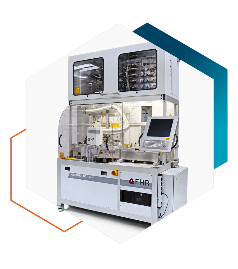

What is PECVD?
Plasma-Enhanced Chemical Vapor Deposition (PECVD) is a vacuum deposition process that uses plasma energy to activate chemical reactions, allowing thin films to be deposited at significantly lower temperatures than conventional chemical vapor deposition (CVD). This makes PECVD well suited for temperature-sensitive substrates while maintaining excellent film quality, uniformity, and process control.
Unlike traditional CVD processes, PECVD enables high-quality coatings with improved conformity, controlled film properties, and excellent repeatability for demanding manufacturing environments.


Typical Applications
Semiconductor Manufacturing
PECVD is widely used in semiconductor manufacturing to deposit high-quality dielectric and passivation films for integrated circuits, MEMS, and advanced packaging. Excellent film uniformity and precise process control make it ideal for sensitive devices and precision wafer fabrication.

Optical Coatings
PECVD enables the deposition of thin dielectric films for optical components used in photonics, infrared optics, and precision imaging systems. The process provides excellent coating uniformity, optical performance, and durability for demanding optical applications.

Thin-Film Solar & Photovoltaics
PECVD plays a critical role in photovoltaic manufacturing by depositing silicon-based dielectric and passivation layers used in advanced solar cells. From thin-film technologies to high-efficiency photovoltaic devices, PECVD supports reliable, high-throughput production with consistent film quality and process stability.

Scalable Manufacturing Solutions
FHR’s PECVD systems are available in multiple platform configurations to support research, pilot production, and high-volume manufacturing. Systems can be configured to meet specific process requirements, substrate sizes, and production objectives.
- Research & Development Systems
Flexible platforms designed for process development, prototyping, and university research. - Pilot Production Systems
Scalable solutions that bridge laboratory development with small-volume manufacturing. - High-Volume Manufacturing Systems
Engineered for consistent throughput, process stability, and industrial-scale thin-film production. - Custom Process Development
Tailored chamber configurations, plasma sources, and process integration designed around unique customer requirements. - Integrated Vacuum Coating Platforms
PECVD modules can be combined with complementary thin-film technologies such as sputtering and evaporation to create complete deposition solutions.
Key Advantages
- Low-temperature deposition for temperature-sensitive materials
- Excellent coating uniformity across complex geometries
- High-quality dense thin films
- Precise control of film thickness and material properties
- Scalable from laboratory research to industrial production
- Supports deposition of a broad range of dielectric, semiconductor, and functional thin films.
Supported Thin-Film Materials
-
High-quality dielectric films for insulation, passivation, optical coatings, and protective layers.
- Silicon Oxide (SiO₂)
- Silicon Nitride (SiNx)
- Silicon Oxynitride (SiON)
- Aluminum Oxide (Al₂O₃)*
-
Engineered for semiconductor devices, MEMS, photonics, and photovoltaic manufacturing.
- Amorphous Silicon (a-Si:H)
- Microcrystalline Silicon (μc-Si)
- Doped Silicon Films
- Silicon Carbide (SiC)*
-
Designed to improve wear resistance, optical performance, barrier properties, and environmental protection.
- Diamond-Like Carbon (DLC)*
- Barrier Coatings
- Optical Dielectric Films
-
Tailored PECVD solutions developed to meet unique materials, substrates, and production requirements.
- Customer-Specific Chemistries
- Process Development Support
- Integrated Deposition Solutions
Why Choose Vital Materials?
- Global engineering and application support
- Proven FHR vacuum coating expertise
- Custom process development
- Integrated thin-film manufacturing solutions
- Worldwide service and technical support