Atomic Layer Deposition (ALD) Systems



What is Atomic Layer Deposition?
Atomic Layer Deposition (ALD) is a thin-film deposition process that deposits materials one atomic layer at a time using sequential, self-limiting chemical reactions. Unlike conventional CVD processes, ALD provides atomic-scale thickness control, exceptional conformality over complex three-dimensional structures, and highly uniform thin films across wafers and large-area substrates.
Because each deposition cycle is self-limiting, ALD enables unmatched precision, repeatability, and film quality for advanced thin-film manufacturing.
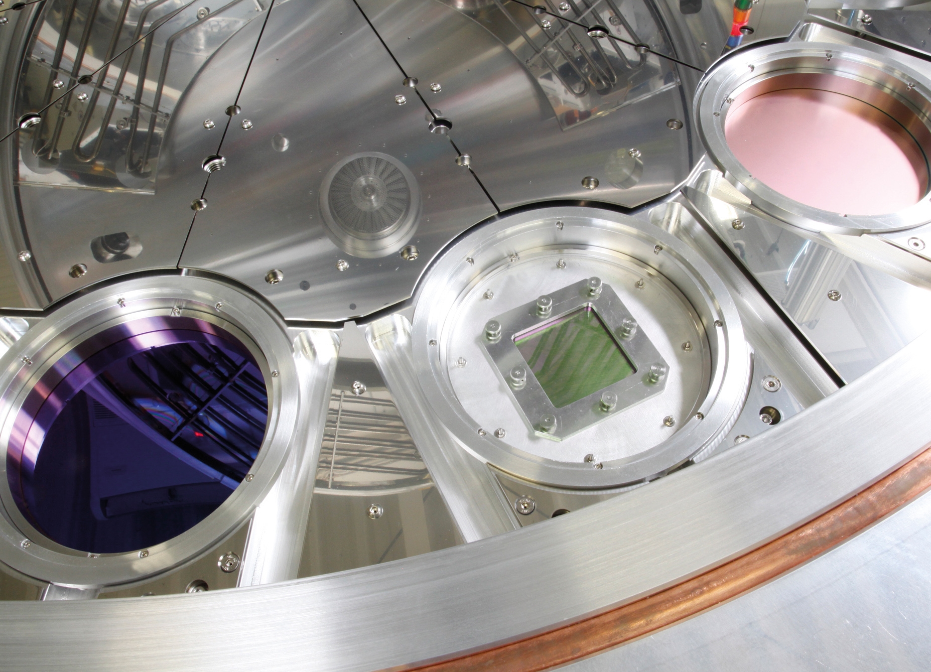

Typical Applications
Semiconductor Manufacturing
High-k dielectrics, gate oxides, passivation layers, and advanced logic devices.
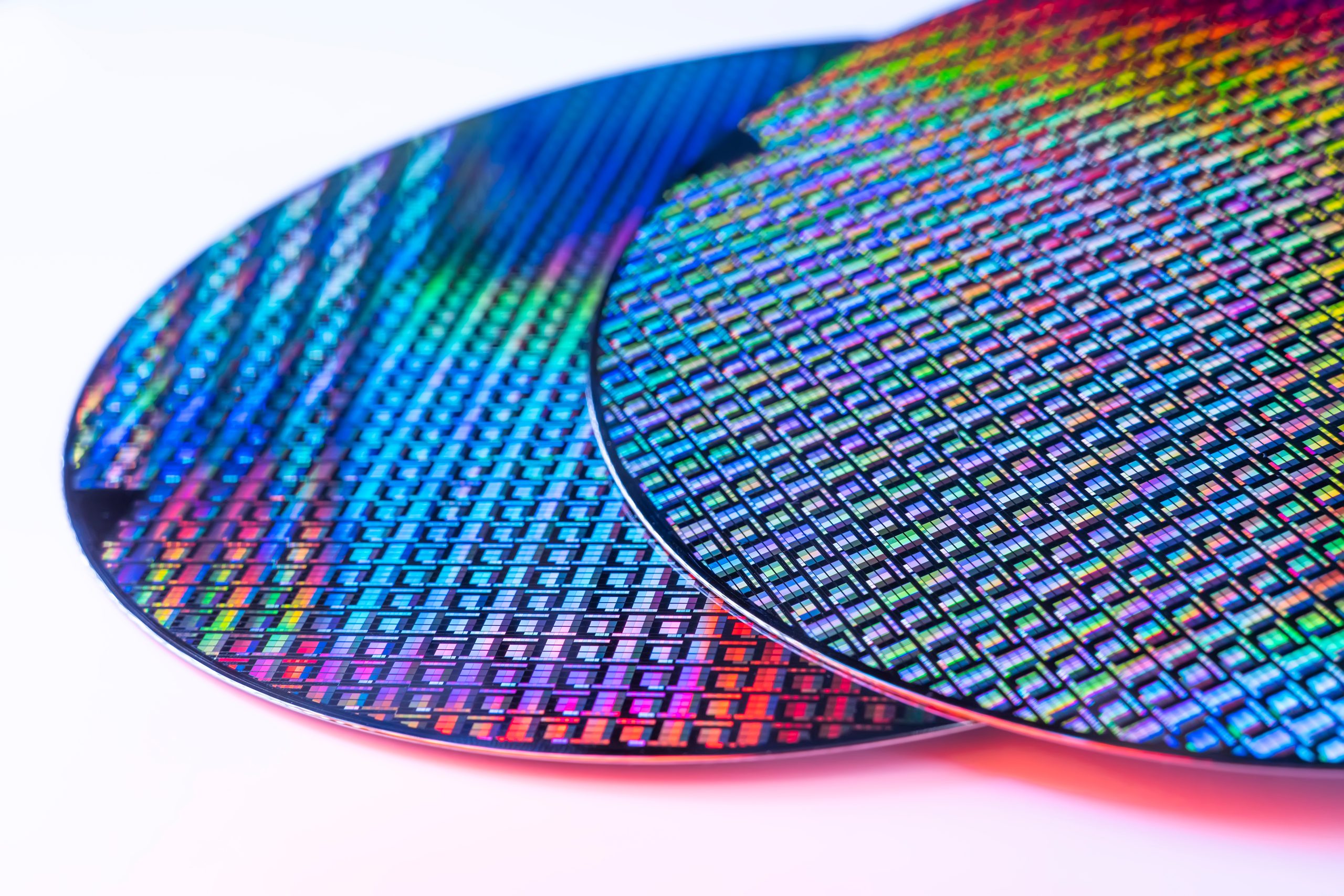
Sensors & Imaging
Conformal coatings for microelectromechanical systems and precision sensor manufacturing.

Photonics & Optics
Waveguides, optical coatings, anti-reflective layers, and photonic devices.
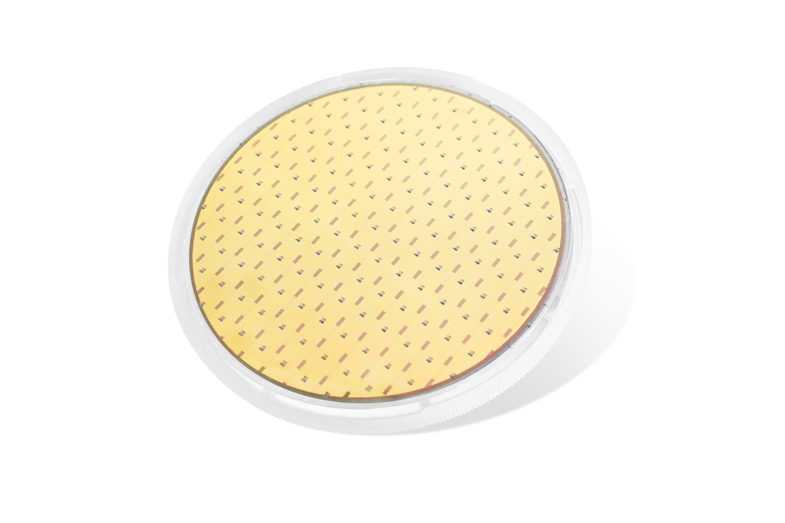
Energy Storage & Clean Energy
Precision thin-film coatings for advanced batteries, photovoltaic technologies, and fuel cell components.

Power Electronics
High-performance dielectric and protective coatings for SiC, GaN, and other wide-bandgap power semiconductor devices.

Scalable Manufacturing Solutions
FHR’s ALD systems are available in flexible platform configurations to support research, process development, pilot production, and high-volume manufacturing. Systems can be configured for specific process requirements, substrate formats, throughput targets, and advanced thin-film applications.
- Research & Development Systems
Flexible platforms designed for materials research, process development, prototyping, and university applications. - Pilot Production Systems
Scalable solutions that bridge laboratory development with small-volume manufacturing and process scale-up. - High-Volume Manufacturing Systems
Production platforms engineered for consistent throughput, process stability, and industrial-scale thin-film deposition. - High-Throughput Spatial ALD Systems
Spatial ALD configurations designed to increase deposition throughput for applications requiring precise, uniform thin-film coatings. - Custom & Integrated Process Platforms
Configurable systems supporting application-specific process requirements and integration with complementary thin-film deposition technologies.
Key Advantages
- Low-temperature deposition for temperature-sensitive materials
- Excellent coating uniformity across complex geometries
- High-quality dense thin films
- Precise control of film thickness and material properties
- Scalable from laboratory research to industrial production
- Supports deposition of a broad range of dielectric, semiconductor, and functional thin films.
Common ALD Thin-Film Materials
-
High-quality dielectric films for insulation, passivation, optical coatings, and protective layers.
- Aluminum Oxide (Al₂O₃)
- Silicon Dioxide (SiO₂)
- Hafnium Oxide (HfO₂)
- Tantalum Oxide (Ta₂O₅)
-
Engineered for semiconductor devices, MEMS, photonics, and photovoltaic manufacturing.
- Titanium Nitride (TiN)
- Aluminum Nitride (AlN)
- Silicon Nitride (SiNx)
- Zinc Oxide (ZnO)
- Zirconium Oxide (ZrO₂)
ALD Precursors & Source Materials
Vital Materials also provides precursor materials for advanced ALD processes, supporting integrated solutions from source materials to thin-film deposition equipment.
Why Choose Vital Materials?
- Atomic-Level Thickness Control
- Deposit films with angstrom-level precision for demanding semiconductor and nanotechnology applications.
- Excellent Step Coverage
- Achieve highly conformal coatings on complex 3D structures, deep trenches, and high aspect ratio features.
- Outstanding Uniformity
- Uniform thin films across wafers and large-area glass substrates for repeatable production.
- Scalable Manufacturing Platforms
- Solutions available for research laboratories, pilot production, and industrial-scale manufacturing.
- Integrated Source-to-Solution Capability
- Combine ALD equipment with Vital’s precursor materials, recycling capabilities, and process expertise.