Germanium Wafers
 Product PDF
Germanium (Ge) Substrates
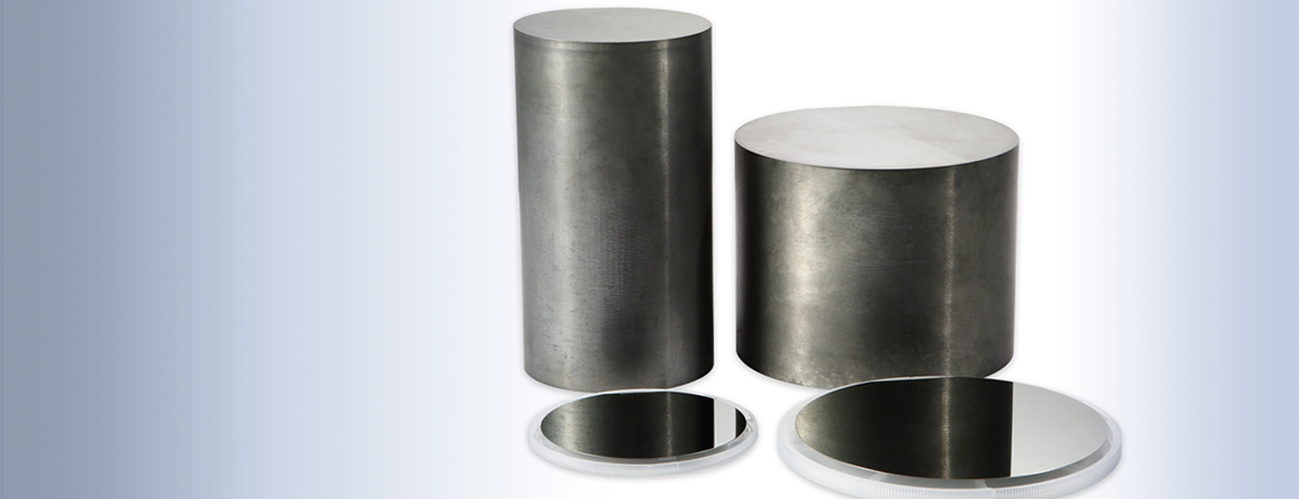
Vital manufactures Low EPD (etch pit density) or even Zero EPD Ge substrates, supplied in diameters from 2" up to 6" with a Resistivity from 0.005 Ω·cm to over 50Ω·cm. Monocrystalline Ge wafers are an important semiconductor substrate material. High quality substrates are used in Concentrator Photovoltaic power stations (CPV), outer-space solar cell panels and ultra-high brightness LEDs.
Market and application
Germanium single crystal wafers are an important semiconductor substrate material. These high-quality substrates are primarily used in CPV, outer-space solar-cell panel and high-bright light-emitting diode applications.
 Custom-made Ge substrates configurations are available upon request.
| Item | Unit | Semiconduct Specifications | |
|---|---|---|---|
| Crystal Growth Method | CZ | ||
| Conduct Type | (n-type) | (p-type) | |
| Dopant | As,Sb | Ga | |
| Diameter | inch | 2",3",4" and 6" | |
| Wafer Orientation | (100)±0.5° | ||
| OF/IF | US,EJ | ||
| Laser Marking | /cm3 | Upon request | |
| Thickness | μm | (175-500)±25 | |
| Resistivity (at RT) | ohm.cm | 0.005-30 | 0.005-0.04 |
| Etch Pit Density (EPD) | /cm2 | - | 0 |
| TTV | μm | ≤15 | ≤15 |
| Warp | μm | ≤25 | ≤25 |
| Backside Ra | μm | <0.1 | <0.1 |
| Surface | Side1/Side2 | E/E, P/E, P/D | |
| Epi-ready | Yes | ||
| Package | Cassette or single wafer container |
||